-
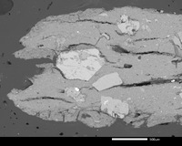
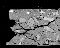 AF ZMT 006 SEM images acquisition
 Backscattered Images acquired by Scanning Electron Microscopy at 50x and 200x magnification. Images from right to left top and bottom surface 1 to 7 at 50 x. Images from 8 to 20 at 200x.
-
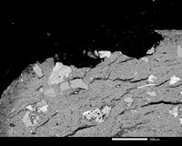 AF ZMT 005 SEM images acquisition
 Backscattered Images acquired by Scanning Electron Microscopy at 50x and 200x magnification. Images from right to left top and bottom surface 1 to 4 at 50 x. Images from 5 to 13 at 200x.
-
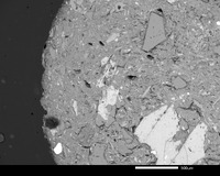 AF ZMT 004 SEM images acquisition
 Backscattered Images acquired by Scanning Electron Microscopy at 50x and 200x magnification. Images from right to left top and bottom surface 1 to 21 at 50 x. Images from 22 to 31 at 200x.
-
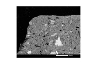 AF ZMT 003 SEM images acquisition
 Backscattered Images acquired by Scanning Electron Microscopy at 50x and 200x magnification. Images from 1 to 8 at 50x. Images from 9 to 36 at 200x
-
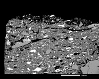
 AF UEN 002 SEM images acquisition
 Backscattered Images acquired by Scanning Electron Microscopy at 50x and 200x magnification.
Images along the surface from left to right: 1 to 5 at 50x
Images from 6 to 12 at 200x
-
 ICP-OES data table - Tatetsuki, Ueno, Zanmochi and Ishida samples
 Data table for ceramic samples from Tatetski and Shimane (Ueno, Zanmochi and Ishida) analysed by Inductive Coupled Plasma Optical Emission Spectroscopy.
-
 AF TTK 010 OM for SEM acquisition
 Optical microphotogrametry specifying areas for SEM images and areas analysed by Scanning Electron Microscopywith Energy Dispersive X-ray.
-
 AF TTK 009 OM for SEM acquisition
 Optical microphotogrametry specifying areas for SEM images and areas analysed by Scanning Electron Microscopywith Energy Dispersive X-ray.
-
 AF TTK 008 OM for SEM acquisition
 Optical microphotogrametry specifying areas for SEM images and areas analysed by Scanning Electron Microscopywith Energy Dispersive X-ray.
-
 AF TTK 007 OM for SEM acquisition
 Optical microphotogrametry specifying areas for SEM images and areas analysed by Scanning Electron Microscopywith Energy Dispersive X-ray.
-
 AF TTK 006 OM for SEM acquisition
 Optical microphotogrametry specifying areas for SEM images and areas analysed by Scanning Electron Microscopywith Energy Dispersive X-ray.
-
 AF TTK 005 OM for SEM acquisition
 Optical microphotogrametry specifying areas for SEM images and areas analysed by Scanning Electron Microscopywith Energy Dispersive X-ray.
-
 AF TTK 003 OM for SEM acquisition
 Optical microphotogrametry specifying areas for SEM images and areas analysed by Scanning Electron Microscopywith Energy Dispersive X-ray.
-
 AF TTK 002 OM for SEM acquisition
 Optical microphotogrametry specifying areas for SEM images and areas analysed by Scanning Electron Microscopywith Energy Dispersive X-ray.
-
 AF TTK 001 OM for SEM acquisition
 Optical microphotogrametry specifying areas for SEM images and areas analysed by Scanning Electron Microscopywith Energy Dispersive X-ray.
-
 AF ISH 007 OM for SEM acquisition
 Optical microphotogrametry specifying areas for SEM images and areas analysed by Scanning Electron Microscopy with Energy Dispersive X-ray.
-
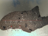
 AF ZMT 006 OM for SEM acquisition
 Optical microphotogrametry specifying areas for SEM images and areas analysed by Scanning Electron Microscopywith Energy Dispersive X-ray.
-
 AF ZMT 005 OM for SEM acquisition
 Optical microphotogrametry specifying areas for SEM images and areas analysed by Scanning Electron Microscopywith Energy Dispersive X-ray.
-
 AF ZMT 004 OM for SEM acquisition
 Optical microphotogrametry specifying areas for SEM images and areas analysed by Scanning Electron Microscopywith Energy Dispersive X-ray.
-
 AF ZMT 003 OM for SEM acquisition
 Optical microphotogrametry specifying areas for SEM images and areas analysed by Scanning Electron Microscopywith Energy Dispersive X-ray.
-
 AF UEN 002 OM for SEM acquisition
 Optical microphotogrametry specifying areas for SEM images and areas analysed by Scanning Electron Microscopy with Energy Dispersive X-ray.
-
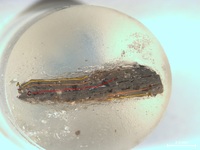
 AF UEN 001 OM for SEM acquisition
 Optical microphotogrametry specifying areas for areas analysed by Scanning Electron Microscopy with Energy Dispersive X-ray.
-
 AF UEN 001 SEM images acquisition
 Backscattered Images acquired by Scanning Electron Microscopy at 50x and 200x magnification.
Images along the surface from left to right from 1 to 6 at 50x; 7 to 16 at 200x; Images also under 17 to 19 at 50x
-
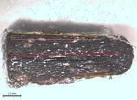
AF UEN 001 SEM EDX processing and modeling
Elemental examination of AF UEN 001 cross section.
-
 AF UEN 001 SEM EDX acquisition
 Elemental chemical composition acquired by Scanning Electron Microscopy with Energy Dispersive X-ray analysis.